- 您现在的位置:买卖IC网 > Sheet目录1994 > DS3232MZ+ (Maxim Integrated Products)IC RTC W/SRAM I2C 8SOIC
DS3232M
±5ppm, I2C Real-Time Clock with SRAM
4
Maxim Integrated
Note 2: Limits are 100% tested at TA = +25°C and TA = +85°C. Limits over the operating temperature range and relevant supply
voltage range are guaranteed by design and characterization. Typical values are not guaranteed.
Note 3: Includes the temperature conversion current (averaged).
Note 4: Does not include RST leakage if VCC < VPF.
Note 5: The parameter tOSF is the period of time the oscillator must be stopped for the OSF flag to be set.
Note 6: The state of RST does not affect the I2C interface or RTC functions.
Note 7: Interface timing shown is for fast-mode (400kHz) operation. This device is also backward-compatible with standard mode
I2C timing.
Note 8: CB = total capacitance of one bus line in picofarads.
Note 9: Guaranteed by design and not 100% production tested.
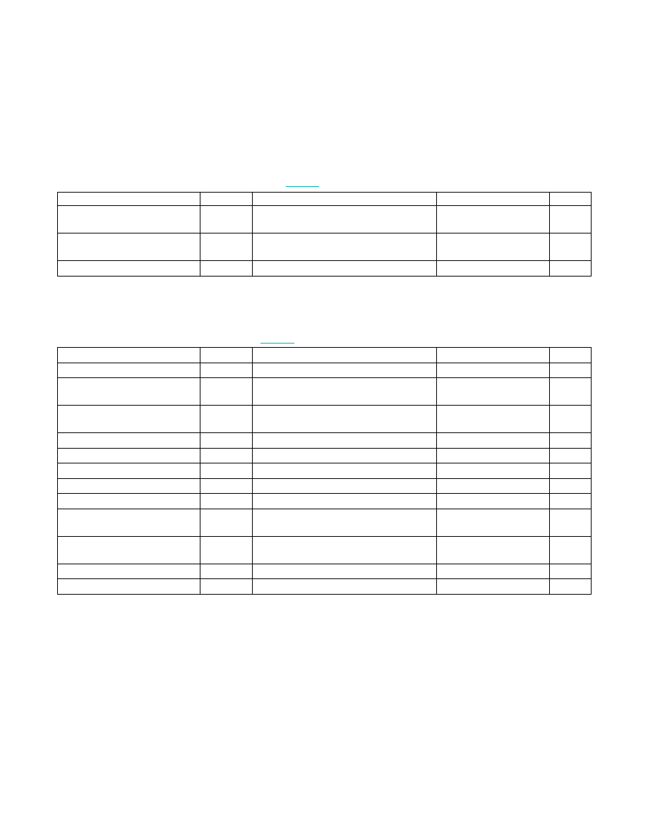
AC ELECTRICAL CHARACTERISTICS—POWER SWITCH
AC ELECTRICAL CHARACTERISTICS—I2C INTERFACE
(VCC or VBAT = +2.3V to +4.5V, TA = -40NC to +85NC, unless otherwise noted. Typical values are at VCC = +3.3V, VBAT = +3.0V, and
PARAMETER
SYMBOL
CONDITIONS
MIN
TYP
MAX
UNITS
VCC Fall Time, VPFMAX to
VPFMIN
tVCCF
300
F
s
VCC Rise Time, VPFMIN to
VPFMAX
tVCCR
0
F
s
Recovery at Power-Up
tREC
(Note 6)
250
300
ms
PARAMETER
SYMBOL
CONDITIONS
MIN
TYP
MAX
UNITS
SCL Clock Frequency
fSCL
0
400
kHz
Bus Free Time Between STOP
and START Conditions
tBUF
1.3
F
s
Hold Time (Repeated) START
Condition
tHD:STA
0.6
F
s
Low Period of SCL
tLOW
1.3
F
s
High Period of SCL
tHIGH
0.6
F
s
Data Hold Time
tHD:DAT
0
0.9
F
s
Data Set-Up Time
tSU:DAT
100
ns
START Set-Up Time
tSU:STA
0.6
F
s
SDA and SCL Rise Time
tR
(Note 8)
20 +
0.1CB
300
ns
SDA and SCL Fall Time
tF
(Note 8)
20 +
0.1CB
300
ns
STOP Set-Up Time
tSU:STO
0.6
F
s
SDA, SCL Input Capacitance
CBIN
(Note 9)
10
pF
发布紧急采购,3分钟左右您将得到回复。
相关PDF资料
DS3232SN#T&R
IC RTC W/TCXO 20-SOIC
DS3234S#
IC RTC W/TCXO 20-SOIC
DS32C35-33#T&R
IC RTC ACCURATE I2C 3.3V 20-SOIC
DS3911T+
IC DAC 10BIT I2C QUAD 14TDFN
DS4000KI/WBGA
IC OSC TCXO 19.44MHZ 24-BGA
DS4026S+WCN
IC OSC TCXO 25MHZ 16-SOIC
DS4100HW+
IC OSC CLOCK 100MHZ 10LCCC
DS4266P+
IC OSC CLOCK 266MHZ 10-LCCC
相关代理商/技术参数
DS3232MZ+TRL
功能描述:实时时钟 RTC/TCMO/MEMS RoHS:否 制造商:Microchip Technology 功能:Clock, Calendar. Alarm RTC 总线接口:I2C 日期格式:DW:DM:M:Y 时间格式:HH:MM:SS RTC 存储容量:64 B 电源电压-最大:5.5 V 电源电压-最小:1.8 V 最大工作温度:+ 85 C 最小工作温度: 安装风格:Through Hole 封装 / 箱体:PDIP-8 封装:Tube
DS3232N
制造商:MAXIM 制造商全称:Maxim Integrated Products 功能描述:Extremely Accurate I2C RTC with Integrated Crystal and SRAM
DS3232S
制造商:Maxim Integrated Products 功能描述:Extremely Accurate I2C RTC
DS3232S-
制造商:MAXIM 制造商全称:Maxim Integrated Products 功能描述:Extremely Accurate I2C RTC with Integrated Crystal and SRAM
DS3232S#
功能描述:实时时钟 Integrated RTC/TCXO/Crystal RoHS:否 制造商:Microchip Technology 功能:Clock, Calendar. Alarm RTC 总线接口:I2C 日期格式:DW:DM:M:Y 时间格式:HH:MM:SS RTC 存储容量:64 B 电源电压-最大:5.5 V 电源电压-最小:1.8 V 最大工作温度:+ 85 C 最小工作温度: 安装风格:Through Hole 封装 / 箱体:PDIP-8 封装:Tube
DS3232S#T&R
制造商:Maxim Integrated Products 功能描述:EXTREMELY ACCURATE I2C RTC 20SOIC W - Tape and Reel 制造商:Maxim Integrated Products 功能描述:DS3232 3V 20P SOIC 制造商:Maxim Integrated Products 功能描述:IC RTC W/TCXO 20-SOIC
DS3232S#T&R
功能描述:实时时钟 Integrated RTC/TCXO/Crystal RoHS:否 制造商:Microchip Technology 功能:Clock, Calendar. Alarm RTC 总线接口:I2C 日期格式:DW:DM:M:Y 时间格式:HH:MM:SS RTC 存储容量:64 B 电源电压-最大:5.5 V 电源电压-最小:1.8 V 最大工作温度:+ 85 C 最小工作温度: 安装风格:Through Hole 封装 / 箱体:PDIP-8 封装:Tube
DS3232SN
制造商:Maxim Integrated Products 功能描述:Extremely Accurate I2C RTC